Photonics found its foundry model, and the effect resembles electronics in the 1980s
Shared process design kits and multi-project wafer runs let a small team design a photonic chip without owning a fab. That is the structural change.

Integrated photonics has advanced steadily for two decades, but the change with the largest practical consequence is organisational rather than physical: the arrival of a working foundry ecosystem.
What the model provides
A photonic foundry offers a stable fabrication process and a process design kit — a library of characterised building blocks with models accurate enough to simulate a circuit before committing to fabrication. Waveguides, couplers, modulators, detectors and phase shifters come with performance data and design rules.
Multi-project wafer runs let several customers share a wafer and its mask cost, reducing the price of a prototype from a fab-scale investment to something a research group or startup can fund.
Why this matters more than any device result
Before this, designing a photonic chip meant either owning a fabrication capability or negotiating a bespoke arrangement with someone who did. Each design cycle was slow and expensive, and knowledge stayed inside the few organisations with facilities.
The foundry model separates design from fabrication, which is precisely the separation that let electronics scale. Design teams can specialise in circuits and systems without capital equipment, and the number of people able to attempt a photonic design rises by orders of magnitude.
The material platforms
Silicon photonics dominates by volume, leveraging CMOS infrastructure. It cannot emit light, so lasers are attached rather than grown, and integration is the persistent challenge.
Indium phosphide provides native light emission and suits transmitters, at higher cost and lower wafer scale.
Silicon nitride offers very low loss and wide transparency, suiting sensing and non-linear applications, without native emission or fast modulation.
Each has a foundry ecosystem, and platform choice is now a design decision made early rather than a consequence of which facility was available.
Where the constraint has moved
Packaging. Coupling light into and out of a chip, aligning fibres to sub-micrometre tolerance, managing thermal load and providing electrical connections often dominates cost — frequently exceeding the die itself.
That is where the field's engineering attention has moved, and it is the most reliable signal that the fabrication problem is, for practical purposes, solved.
This article was produced by the LasersNews AI desk and reviewed by our editors.
Related reading
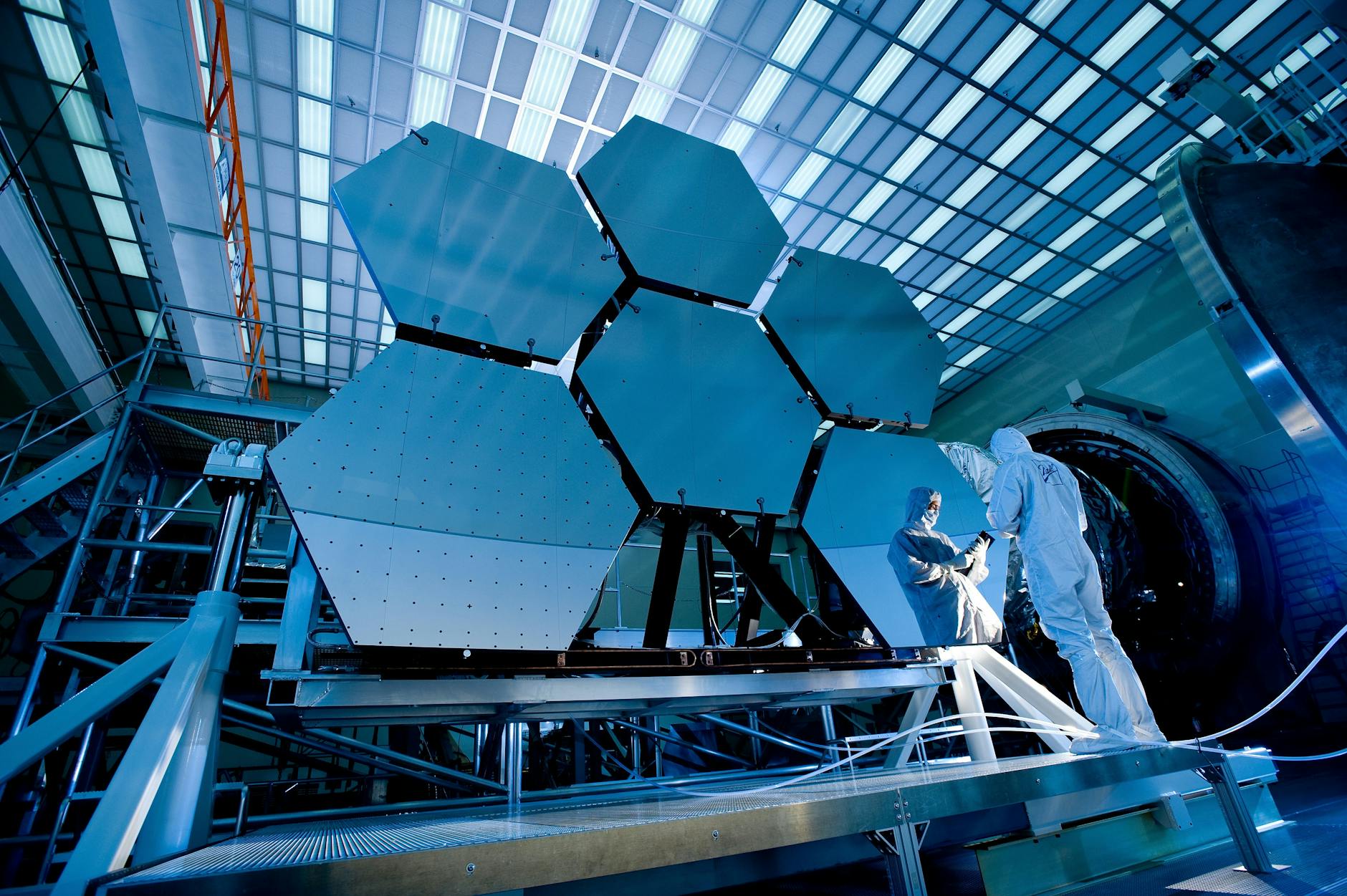
Integrated photonics narrows the gap between laboratory result and manufacturable part
Foundry access and standardised process design kits are doing for photonics roughly what they did for electro…
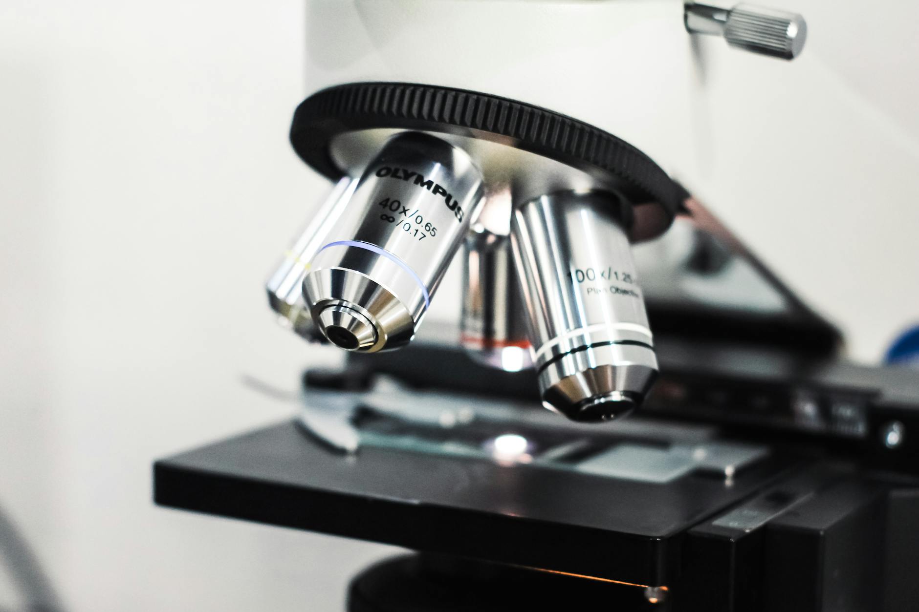
Metasurface optics are running into the manufacturing question
Flat lenses built from sub-wavelength structures work. Producing them at volume, at yield, with the tolerance…

Frequency combs are becoming components rather than experiments
A comb links optical frequencies to microwave references with extraordinary precision. Microresonator version…