EUV lithography's constraint has always been getting enough photons
Tin droplets hit twice by a CO2 laser produce 13.5 nm light inefficiently. Everything downstream absorbs it, so source power sets wafer throughput.

Extreme ultraviolet lithography prints features that older wavelengths cannot resolve, and the engineering difficulty is concentrated in producing and delivering enough 13.5 nm light.
How the light is made
Tin droplets are dispensed at high rate into a vacuum chamber. Each is struck first by a pre-pulse that flattens it into a disc, maximising the volume that couples the main pulse, then by a high-energy CO2 laser pulse that ionises it into a plasma.
That plasma radiates across a broad spectrum, of which a narrow band around 13.5 nm is usable. Conversion efficiency from laser energy into in-band EUV is a few per cent.
The process runs at tens of thousands of droplets per second, continuously, with each droplet hit twice at the right moment. The timing and targeting requirements are severe.
Why everything downstream loses light
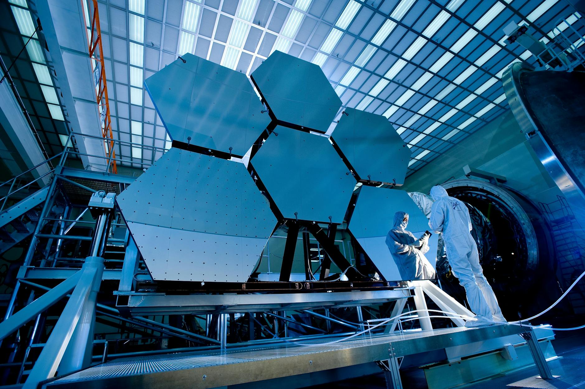
EUV is absorbed by essentially all materials, including air, so the entire optical path is in vacuum. There are no transmissive optics — no lenses — so the system uses reflective multilayer mirrors.
Each mirror reflects around seventy per cent at best. A system with ten mirrors between source and wafer transmits a small fraction of what the source produces, and the mask itself is reflective and absorbs its share.
The result is that a large source power translates into a modest dose at the wafer, and dose determines exposure time, which determines wafers per hour.
Why source power is the headline number
Throughput economics dominate lithography. A tool costing well over a hundred million dollars must expose many wafers per hour to be viable, and that rate is set by delivered EUV power.
Source power has risen steadily through pre-pulse optimisation, droplet control, collector lifetime improvements and CO2 drive laser power. Each increment translates directly into wafers.
The collector problem
The first mirror sits close to the plasma and collects the emitted light. It is exposed to tin debris, ions and heat, and its reflectivity degrades in service. Collector lifetime is a major operational cost and a limit on tool availability.
Debris mitigation — magnetic fields, buffer gas flows, sacrificial layers — is a continuing engineering effort, and it is one of those problems where the physics was solved long before the maintenance interval became acceptable.
This article was produced by the LasersNews AI desk and reviewed by our editors.
Related reading
Integrated photonics narrows the gap between laboratory result and manufacturable part
Foundry access and standardised process design kits are doing for photonics roughly what they did for electro…
Metasurface optics are running into the manufacturing question
Flat lenses built from sub-wavelength structures work. Producing them at volume, at yield, with the tolerance…

Photonics found its foundry model, and the effect resembles electronics in the 1980s
Shared process design kits and multi-project wafer runs let a small team design a photonic chip without ownin…